- 您现在的位置:买卖IC网 > Sheet目录983 > HI5805EVAL1 (Intersil)EVALUATION PLATFORM HI5805
�� �
�
�Application� Note� 9707�
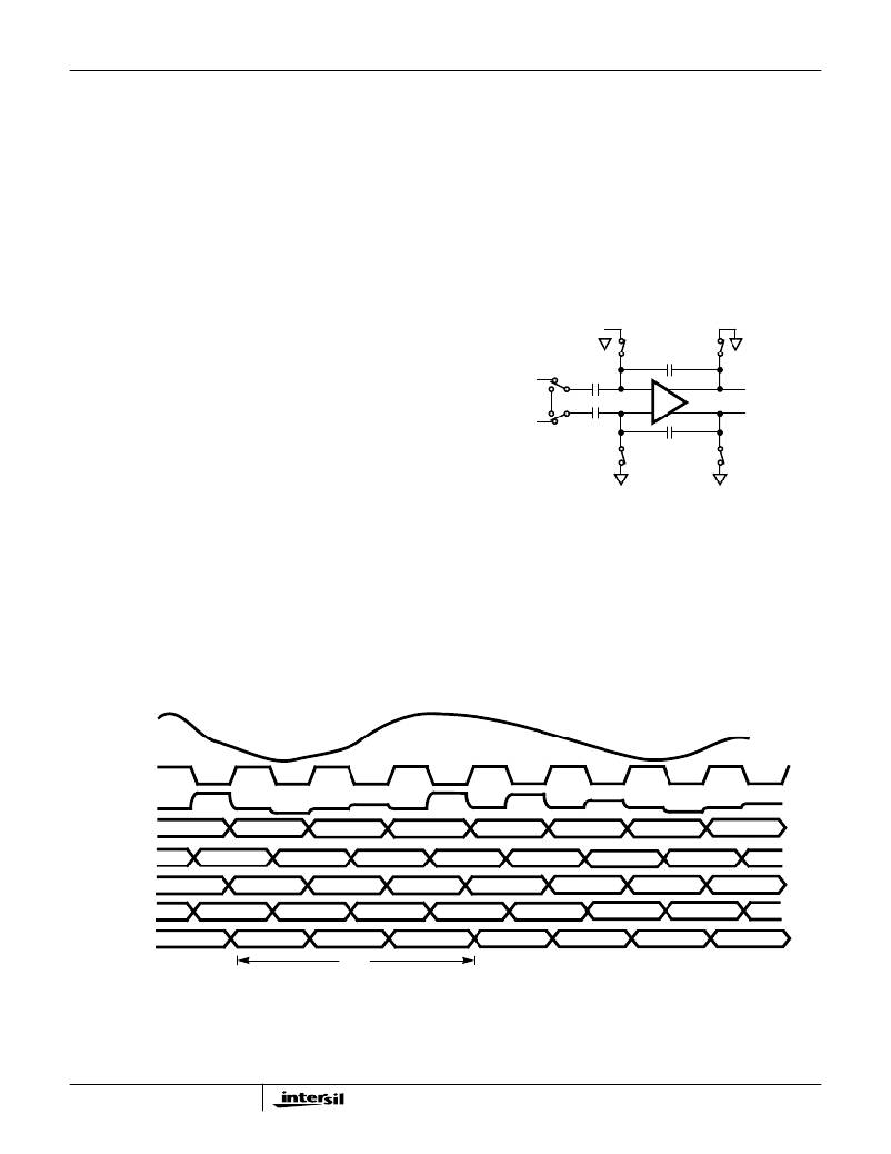
�HI5805� A/D� Theory� of� Operation�
�The� HI5805� is� a� 12-bit� fully� differential� sampling� pipelined�
�A/D� converter� with� digital� error� correction.� Figure� 1� depicts�
�the� circuit� for� the� converters� front-end� differential-in-�
�differential-out� sample-and-hold� (S/H).� The� sampling�
�switches� are� controlled� by� internal� sampling� clock� signals�
�which� consist� of� two� phase� non-overlapping� clock� signals,� φ� 1�
�and� φ� 2,� derived� from� the� master� clock� (CLK)� driving� the�
�converter.� During� the� sampling� phase,� φ� 1,� the� input� signal� is�
�applied� to� the� sampling� capacitors,� C� S� .� At� the� same� time� the�
�holding� capacitors,� C� H� ,� are� discharged� to� analog� ground.� At�
�the� falling� edge� of� φ� 1� the� input� analog� signal� is� sampled� on�
�the� bottom� plates� of� the� sampling� capacitors.� In� the� next�
�clock� phase,� φ� 2,� the� two� bottom� plates� of� the� sampling�
�the� result� that� alternate� stages� in� the� pipeline� will� perform� the�
�same� operation.� The� output� of� each� of� the� three� identical� four-�
�bit� subconverter� stages� is� a� four-bit� digital� word� containing� a�
�supplementary� bit� to� be� used� by� the� digital� error� correction�
�logic.� The� output� of� each� subconverter� stage� is� input� to� a� digital�
�delay� line� which� is� controlled� by� the� internal� clock.� The� function�
�of� the� digital� delay� line� is� to� time� align� the� digital� outputs� of� the�
�three� identical� four-bit� subconverter� stages� with� the�
�corresponding� output� of� the� fourth� stage� flash� converter� before�
�inputting� the� sixteen� bit� result� into� the� digital� error� correction�
�logic.� The� digital� error� correction� logic� uses� the� supplementary�
�bits� to� correct� any� error� that� may� exist� before� generating� the�
�final� twelve-bit� digital� data� output� (D0-D11)� of� the� converter.�
�capacitors� are� connected� together� and� the� holding� capacitors�
�are� switched� to� the� op� amp� output� nodes.� The� charge� then�
�redistributes� between� C� S� and� C� H� ,� completing� one� sample-�
�and-hold� cycle.� The� output� of� the� sample-and-hold� is� a� fully-�
�differential,� sampled-data� representation� of� the� analog� input.�
�The� circuit� not� only� performs� the� sample-and-hold� function,�
�but� can� also� convert� a� single-ended� input� to� a� fully-differential�
�output� for� the� converter� core.� During� the� sampling� phase,� the�
�V� IN� +�
�V� IN� -�
�φ� 1�
�φ� 2�
�φ� 1�
�C� S�
�C� S�
�φ� 1�
�φ� 1�
�C� H�
�-� +�
�+� -�
�C� H�
�φ� 1�
�φ� 1�
�V� OUT� +�
�V� OUT� -�
�V� IN� pins� see� only� the� on-resistance� of� the� switches� and� C� S� .�
�The� relatively� small� values� of� these� components� result� in� a�
�typical� full� power� input� bandwidth� of� 100MHz� for� the� converter.�
�As� illustrated� in� the� HI5805� Functional� Block� Diagram� and� the�
�timing� diagram� contained� Figure� 2,� three� identical� pipeline�
�subconverter� stages,� each� containing� a� four-bit� flash� converter,�
�a� four-bit� digital-to-analog� converter� and� an� amplifier� with� a�
�voltage� gain� of� 8,� follow� the� S/H� circuit� with� the� fourth� stage�
�being� only� a� 4-bit� flash� converter.� Each� converter� stage� in� the�
�pipeline� will� be� sampling� in� one� phase� and� amplifying� in� the�
�other� clock� phase.� Each� individual� sub-converter� clock� signal� is�
�offset� by� 180� degrees� from� the� previous� stage� clock� signal,� with�
�ANALOG�
�INPUT�
�FIGURE� 1.� ANALOG� INPUT� SAMPLE-AND-HOLD�
�Because� of� the� pipeline� nature� of� this� converter,� the� digital�
�data� representing� an� analog� input� sample� is� presented� on�
�the� digital� data� output� bus� on� the� 3rd� cycle� of� the� clock� after�
�the� analog� sample� is� taken.� This� delay� is� speci?ed� as� the�
�data� latency.� After� the� data� latency� time,� the� data�
�representing� each� succeeding� analog� sample� is� output� on�
�the� following� clock� pulse.� The� output� data� is� synchronized� to�
�the� external� sampling� clock� with� a� data� latch� and� is�
�presented� in� offset� binary� format.�
�CLOCK�
�INPUT�
�S� N-1�
�H� N-1�
�S� N�
�H� N�
�S� N+1�
�H� N+1�
�S� N+2�
�H� N+2�
�S� N+3�
�H� N+3�
�S� N+4�
�H� N+4�
�S� N+5�
�H� N+5�
�S� N+6�
�H� N+6�
�INPUT�
�S/H�
�1ST�
�STAGE�
�2ND�
�STAGE�
�3RD�
�STAGE�
�4TH�
�STAGE�
�DATA�
�OUTPUT�
�B� 2,� N-2�
�B� 4,� N-3�
�B� 1,� N-1�
�B� 3,� N-2�
�D� N-3�
�B� 2,� N-1�
�B� 4,� N-2�
�B� 1,� N�
�B� 3,� N-1�
�D� N-2�
�B� 2,� N�
�B� 4,� N-1�
�B� 1,� N+1�
�B� 3,� N�
�D� N-1�
�B� 2,� N+1�
�B� 4,� N�
�B� 1,� N+1�
�B� 3,� N+1�
�D� N�
�B� 2,� N+1�
�B� 4,� N+1�
�B� 1,� N+2�
�B� 3,� N+1�
�D� N+1�
�B� 2,� N+2�
�B� 4,� N+1�
�B� 1,� N+3�
�B� 3,� N+2�
�D� N+1�
�B� 2,� N+3�
�B� 4,� N+2�
�B� 1,� N+7�
�B� 3,� N+3�
�D� N+2�
�NOTES:�
�t� LAT�
�1.� S� N� :� N-th� sampling� period.�
�2.� H� N� :� N-th� holding� period.�
�3.� B� M� ,� N� :� M-th� stage� digital� output� corresponding� to� N-th� sampled� input.�
�4.� D� N� :� Final� data� output� corresponding� to� N-th� sampled� input.�
�FIGURE� 2.� HI5805� INTERNAL� CIRCUIT� TIMING�
�3-2�
�发布紧急采购,3分钟左右您将得到回复。
相关PDF资料
HI5828EVAL2
EVALUATION PLATFORM HI5828
HI5960SOICEVAL1
EVALUATION PLATFORM SOIC HI5960
HI7188EVAL
EVALUATION PLATFORM HI7188
HI7190EVAL
EVALUATION PLATFORM HI7190
HJ4-L-DC12V
RELAY GEN PURPOSE 4PDT 5A 12V
HL2-HP-AC100V-F
RELAY GEN PURPOSE DPDT 10A 100V
HLM01510Z16K50JJ
RES 16.5K OHM 15W 5% WW
HMC1043-DEMO
DEMONSTRATION BOARD FOR HMC1043
相关代理商/技术参数
HI5806IB
制造商:Rochester Electronics LLC 功能描述:- Bulk
HI5808
制造商:INTERSIL 制造商全称:Intersil Corporation 功能描述:12-Bit, 9MSPS A/D Converter
HI5808_01
制造商:INTERSIL 制造商全称:Intersil Corporation 功能描述:12-Bit, 9MSPS A/D Converter
HI5808BIB
制造商:INTERSIL 制造商全称:Intersil Corporation 功能描述:12-Bit, 9MSPS A/D Converter
HI5808BIBR4499
制造商:Rochester Electronics LLC 功能描述:- Bulk 制造商:Harris Corporation 功能描述:
HI5808BIBS2503
制造商:Rochester Electronics LLC 功能描述:- Bulk
HI5808EVAL1
制造商:INTERSIL 制造商全称:Intersil Corporation 功能描述:12-Bit, 10 MSPS A/D Converter
HI5810
制造商:INTERSIL 制造商全称:Intersil Corporation 功能描述:CMOS 10 Microsecond, 12-Bit, Sampling A/D Converter with Internal Track and Hold